
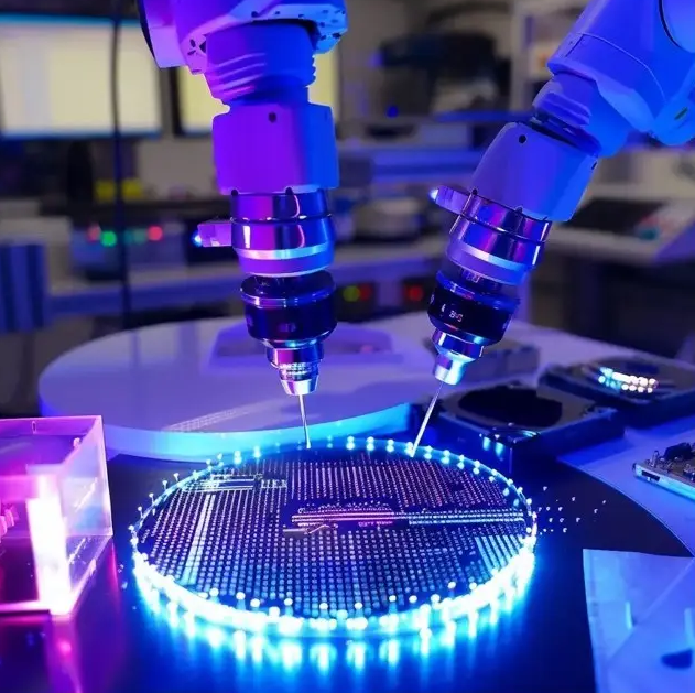
Why we use IR Curing for Wafer Processing
In semiconductor fab, “clean” isn’t just a goal—it’s everything. If you leave even a tiny bit of residue behind during drying or curing, you’ve got a problem. That’s why we lean on precision IR sensors and emitters. It lets us ditch the chemical solvents and combustion heaters entirely. Forget about heating the air. Most people think of ovens, where you heat up the air and hope it transfers to the wafer. It’s slow. It’s clunky. IR is different. It uses electromagnetic radiation to shake up the molecules inside the substrate itself. It’s instant. Plus, you don’t have heating elements burning off gunk into your cleanroom air. If you’re trying to hit “green” mandates or keep metallic contamination out of the room, this is pretty much the only way to go. Hitting the target, not the whole room. Here’s the cool part: we can tune the wavelength. Instead of baking the entire wafer carrier, we target the specific absorption bands of the adhesive or photoresist. You’re heating exactly what needs to be heated. It saves a ton of energy. You aren’t wasting power warming up a giant metal chassis just to cure one 300mm wafer. And because the modules are so compact, you can rip out a massive convection oven and reclaim your floor space. Your HVAC system will thank you, too. The catch (because there’s always a catch). High-intensity IR packs a punch. That’s great for getting wafers through the line faster, but it makes thermal management a bit of a tightrope walk. If your sensors are off by even a hair, you’ll get local hotspots. And hotspots lead to warped wafers. To stop that from happening, you’ve got to pair these emitters with high-speed PID controllers to keep the temperature from spiking. One last tip: don’t cheap out on the wiring. Use shielded cabling. If you don’t, EMI noise will leak into your sensors and mess with your readings. It’s a small detail, but it’s the difference between a perfect batch and a bin full of scrap.